Printed Circuit Boards
Posted by willpost
|
Printed Circuit Boards July 24, 2008 01:20PM |
Registered: 15 years ago Posts: 1 |
Instead of trying to fabricate a circuit board on the spot and have perpetual issues with warping and conductivity, would it be better to build something that can mill and shape circuit boards? We don't require the Laser Printer or Injket to fabricate the paper before printing on it, so maybe it's asking too much for one machine to make the board and the circuit.
The boards could be a standard size, loaded into a cartridge, and then the machine would pull one out, mill the design, drill holes, and trim to shape. I'd go for laser but that would be a limiting factor with making copies of copies.
Then we can worry later about a second machine to fabricate the blank boards. It would probably involve bonding copper foil to a substrate or electroplating it directly.
For reference, are some Google Books on manufacturing circuit boards, including the copper foil process:
Printed Circuit Board Materials Handbook (1997)
[books.google.com]
Printed Circuit Assembly Manufacturing (1987)
[books.google.com]
Edited 1 time(s). Last edit at 07/24/2008 01:22PM by willpost.
|
Re: Printed Circuit Boards July 24, 2008 08:48PM |
Registered: 15 years ago Posts: 251 |
Greetings willpost, et al,
I've had similar thoughts, and this is why I'm (starting to) design my RepStrap to be a more rigid mechanism (and a bit more travel for the axes, esp the horizontal ones.) FYI, there are some plastic anti-backlash Acme nuts available from: [www.dumpstercnc.com]
Both metric and inch threads. I'm seriously considering using these instead of generic threaded rod.
Ideally, I'd like something a bit stronger than a Dremel tool for the spindle. I'm wondering if a router could be made to serve, likely with some supplementary bearings to handle longer toolstrings than a typical router bit (e.g. a chuck for drillbits.) I'd really like an R-8 taper spindle, but that would probably cost too much.
-- Larry
|
Re: Printed Circuit Boards July 24, 2008 11:24PM |
Registered: 15 years ago Posts: 1 |
|
Re: Printed Circuit Boards July 25, 2008 04:06AM |
Registered: 16 years ago Posts: 174 |
Others have been able to successfully mill PCBs:
[forums.reprap.org]
Only problem is milling head vibration, which is a problem that is easily solved.
The question is, is it cheaper to produce blank boards or to buy them?
[forums.reprap.org]
Only problem is milling head vibration, which is a problem that is easily solved.
The question is, is it cheaper to produce blank boards or to buy them?
|
Re: Printed Circuit Boards July 25, 2008 06:26AM |
Registered: 16 years ago Posts: 361 |
Quote
The question is, is it cheaper to produce blank boards or to buy them?
I think I'd probably have to go for the 'buy' option there... making your own boards may well be cheaper, but at what loss of quality and durability? IT'll be one of those problems solved 'one day', but given the availablility of perfectly adequate raw material right now, I don't see the rush.
It has just occurred to me that it might be quite cool to be able to print off a solderless breadboard though.
|
Re: Printed Circuit Boards August 01, 2008 01:01PM |
Registered: 15 years ago Posts: 1 |
getting circuit boards made has, in my experience, been the easiest part of the process - it doesn't take much of a CNC machine to produce one - the sherline class machines do it just fine. The RepRap is in my way of thinking just a specialized (or evolved maybe?) form of CNC machine. And there are lots of companies out there that can produce PCBs relatively inexpensively.
I use my CNC machine for PCB prototyping and I like the fact that I can produce a board right now and test it - so even though it probably doesn't save me much in money, the time aspect is of great value. If/when I need a run of pcb's I will likely send them to a fab house. Down the road of course I'd like to be able to start with nothing and produce a working board from nothing more than a board layout and a reprap - I think we'll need to go through a few intermediate steps before we get to that obviously desirable end goal.
I'd be interested in seeing the RepRap used for direct application of solder paste and potentially even simple pick and place operations. Using the RepRap to apply solder paste seems like a natural fit because it is already prepared for gel/paste type of delivery. I'm not sure what it would take for a RepRap to read gerber files - ideas? Does this seem plausible or does anyone else think this is a good idea?
|
Re: Printed Circuit Boards August 01, 2008 02:37PM |
Registered: 17 years ago Posts: 370 |
hyperk Wrote:
-------------------------------------------------------
> I'm not sure what it would take
> for a RepRap to read gerber files
Not much. You can already get gerber->gcode converters easily, and it should be easy to interpolate the lines for additive fabrication. Of course, it will take a dedicated programmer some time to do it right, but the technical hurdles aren't high. I think it will be much more difficult to determine an effective way of actually producing conductive traces.
|
Re: Printed Circuit Boards August 01, 2008 06:56PM |
Registered: 17 years ago Posts: 550 |
okay buying the pcbs from the rrf store costs what? ~$4/pcb ?
And its tinned, lacquered and silkscreened
As long as I can't do that at home for less, I don't think twice
Don't get me wrong,
it's good to know that I can mill prototypes of boards if I need to,
but if there are readymade pcbs available with a really good quality,
I'm not the one that would build the pcbs myself.
Go and buy at the rrf store,
even if they are (I don't know I guess they are not) costlier than making the boards yourself.
See it as "donation to the rrf-project"
'sid
|
Re: Printed Circuit Boards August 01, 2008 07:20PM |
Registered: 17 years ago Posts: 370 |
sid Wrote:
-------------------------------------------------------
> okay buying the pcbs from the rrf store costs
> what? ~$4/pcb ?
> And its tinned, lacquered and silkscreened
> As long as I can't do that at home for less, I
> don't think twice
Agreed. However, I think the goal is to make printing circuits just as simple as clicking "buy" in the RRRF store is right now, and a good deal faster than shipping them.
One of the uses I'd like to develop for my mill/RepStrap is milling circuit boards. As several others have pointed out, this is really useful for prototyping or one-off production. I'll do just fine milling them for now, but if someone develops a trace-laying RepRap head, I'd switch to that in a heartbeat. The more dust I can avoid generating, the happier I'll be.
|
Printed Circuit Boards August 03, 2008 03:24PM |
Hello. I am new to pcbs. I am working on something, where I need to develop a pcb design for interfacing several devices. Hopefully, someone here knows the blackfin controller and the surveyor bot. What I need to do is design a pcb to house the blackfin, an IMU sensor, and an ADC converter. I have no idea on how to start. Any help or direction is greatly appreciated!
|
Re: Printed Circuit Boards August 03, 2008 04:42PM |
Registered: 17 years ago Posts: 370 |
liam Wrote:
-------------------------------------------------------
> Hello. I am new to pcbs. I am working on
> something, where I need to develop a pcb design
> for interfacing several devices. Hopefully,
> someone here knows the blackfin controller and the
> surveyor bot. What I need to do is design a pcb to
> house the blackfin, an IMU sensor, and an ADC
> converter. I have no idea on how to start. Any
> help or direction is greatly appreciated!
Try reading the tutorials for Eagle PCB design software. Blackfin is a good uC, but much too heavy duty for what we're doing here. I use it at work.
*back on topic*
|
Re: Printed Circuit Boards August 03, 2008 07:17PM |
Registered: 17 years ago Posts: 370 |
Interesting, just came across this story in Hack a Day: [www.hackaday.com]
While it is less than ideal, getting a laser diode that can etch black spraypaint may be easier than trying to get a working milling head.
Both processes are messy - milling gets fine dust *everywhere*, but with etching you need to work with potentially hazardous chemicals.
While it is less than ideal, getting a laser diode that can etch black spraypaint may be easier than trying to get a working milling head.
Both processes are messy - milling gets fine dust *everywhere*, but with etching you need to work with potentially hazardous chemicals.
|
Re: Printed Circuit Boards August 03, 2008 11:50PM |
Registered: 15 years ago Posts: 152 |
Kyle Corbitt Wrote:
-------------------------------------------------------
> Interesting, just came across this story in Hack a
> Day:
> [www.hackaday.com]
> rinted-circuit-boards/
>
> While it is less than ideal, getting a laser diode
> that can etch black spraypaint may be easier than
> trying to get a working milling head.
>
> Both processes are messy - milling gets fine dust
> *everywhere*, but with etching you need to work
> with potentially hazardous chemicals.
It's not that hard to design containment systems, like a vacuum on the milling head, etc. I think the main considerations should be cost, speed, complexity, and materials and equipment used.
|
Re: Printed Circuit Boards August 04, 2008 02:08AM |
Registered: 15 years ago Posts: 37 |
Crackpot idea:
long length of 'fishtank tube' one end positioned close to the milling head other attached to a vacuum cleaner
Disclaimer: While the operation of the the VC may be a mystery the knowledge of the existence of said VC in the household should be know, but is totally deniable.
long length of 'fishtank tube' one end positioned close to the milling head other attached to a vacuum cleaner
Disclaimer: While the operation of the the VC may be a mystery the knowledge of the existence of said VC in the household should be know, but is totally deniable.
|
Re: Printed Circuit Boards August 04, 2008 02:20PM |
Registered: 15 years ago Posts: 152 |
xsainnz Wrote:
-------------------------------------------------------
> Crackpot idea:
>
> long length of 'fishtank tube' one end positioned
> close to the milling head other attached to a
> vacuum cleaner
That's not a crackpot idea; in fact, that's pretty much exactly what I had in mind. I suggest we come up with some way to discredit the milling option, though, so we can have an excuse to use lasers.
-------------------------------------------------------
> Crackpot idea:
>
> long length of 'fishtank tube' one end positioned
> close to the milling head other attached to a
> vacuum cleaner
That's not a crackpot idea; in fact, that's pretty much exactly what I had in mind. I suggest we come up with some way to discredit the milling option, though, so we can have an excuse to use lasers
.
|
Re: Printed Circuit Boards August 04, 2008 03:39PM |
Registered: 17 years ago Posts: 370 |
Joshua Merchant Wrote:
-------------------------------------------------------
> It's not that hard to design containment systems,
> like a vacuum on the milling head, etc. I think
> the main considerations should be cost, speed,
> complexity, and materials and equipment used.
Haha, for the record I've never seen a milling setup that didn't produce a certain amount of dust/scrap, no matter how well set up the vacuum is. I've never seen how professionals do it though.
Joshua Merchant Wrote:
-------------------------------------------------------
> I suggest we come
> up with some way to discredit the milling option,
> though, so we can have an excuse to use lasers.
FFF is a technology that is exponentially more useful (imho) than laser cutting. But it just doesn't have that "dude, laser!" factor... that's why we need both.
-------------------------------------------------------
> It's not that hard to design containment systems,
> like a vacuum on the milling head, etc. I think
> the main considerations should be cost, speed,
> complexity, and materials and equipment used.
Haha, for the record I've never seen a milling setup that didn't produce a certain amount of dust/scrap, no matter how well set up the vacuum is. I've never seen how professionals do it though.
Joshua Merchant Wrote:
-------------------------------------------------------
> I suggest we come
> up with some way to discredit the milling option,
> though, so we can have an excuse to use lasers
.FFF is a technology that is exponentially more useful (imho) than laser cutting. But it just doesn't have that "dude, laser!" factor... that's why we need both
.
|
Re: Printed Circuit Boards August 04, 2008 04:45PM |
Registered: 15 years ago Posts: 152 |
Kyle Corbitt Wrote:
-------------------------------------------------------
> Haha, for the record I've never seen a milling
> setup that didn't produce a certain amount of
> dust/scrap, no matter how well set up the vacuum
> is. I've never seen how professionals do it
> though.
You can still contain the entire thing with a really innovative contraption. I call it a "Bawcks 1.0". Perhaps the contraption's name should use an 'o' instead of 'aw' and an 'x' instead of the 'cks'... naw.
> FFF is a technology that is exponentially more
> useful (imho) than laser cutting. But it just
> doesn't have that "dude, laser!" factor... that's
> why we need both.
I was actually referring to the use of lasers for the black spraypaint etching described at Hack A Day.
-------------------------------------------------------
> Haha, for the record I've never seen a milling
> setup that didn't produce a certain amount of
> dust/scrap, no matter how well set up the vacuum
> is. I've never seen how professionals do it
> though.
You can still contain the entire thing with a really innovative contraption. I call it a "Bawcks 1.0". Perhaps the contraption's name should use an 'o' instead of 'aw' and an 'x' instead of the 'cks'... naw.
> FFF is a technology that is exponentially more
> useful (imho) than laser cutting. But it just
> doesn't have that "dude, laser!" factor... that's
> why we need both
.I was actually referring to the use of lasers for the black spraypaint etching described at Hack A Day.
|
Re: Printed Circuit Boards August 06, 2008 01:51PM |
Registered: 16 years ago Posts: 174 |
You'd need something bigger than fish tank tube, it might get clogged too easily. A better option might be to spray water on the milling head to prevent copper dust from getting in the air like they do with rock cutters. Although spraying water brings up some more problems...
Crackpot idea: negatively charge the board and put a positively charged plate on the milling head to attract away the negatively charged dust.
Any way, most mills I have seen have a blower to prevent the dust from interfering with the work piece. This may not be necessary considering the amount of dust generated.
Why lasers? The laser technique still requires you to etch the boards in ferric chloride. The milling head technique allows you to skip this step. This is advantageous if you want to have another toolhead work on the board, like a pick and place toolhead.( [forums.reprap.org] )
|
Re: Printed Circuit Boards August 06, 2008 03:28PM |
Registered: 17 years ago Posts: 370 |
Gene Hacker Wrote:
-------------------------------------------------------
> You'd need something bigger than fish tank tube,
> it might get clogged too easily. A better option
> might be to spray water on the milling head to
> prevent copper dust from getting in the air like
> they do with rock cutters. Although spraying water
> brings up some more problems...
>
> Crackpot idea: negatively charge the board and put
> a positively charged plate on the milling head to
> attract away the negatively charged dust.
>
> Any way, most mills I have seen have a blower to
> prevent the dust from interfering with the work
> piece. This may not be necessary considering the
> amount of dust generated.
>
> Why lasers? The laser technique still requires you
> to etch the boards in ferric chloride. The milling
> head technique allows you to skip this step. This
> is advantageous if you want to have another
> toolhead work on the board, like a pick and place
> toolhead.(
> [forums.reprap.org] )
I'm not sure that the laser technique is better, just that it is an alternative to be explored. Possible advantages include a cheaper, smaller, and safer head (a focused laser diode that can vaporize black paint is probably less dangerous than a dremel tool). It is also quieter, and potentially better contained in that it doesn't get dust everywhere. But you're right, it has some big drawbacks as well. I'm going to start with milling myself.
|
Re: Printed Circuit Boards August 21, 2008 02:43AM |
Registered: 16 years ago Posts: 900 |
Alternatives....
Make a pen holding tool head and draw a photo mask onto pre sensitized board, then expose, develop and etch in the usual way. (Use disposable drawing pens for fine lines and permanent pigment)
Make a focused and collimated UV LED tool head and photo plot your pre sensitised board, then expose, develop and etch in the usual way.
Doing either/both of the above removes alignment issues providing you plot from a corner origin that you can reposition your board accurately to. You will also be able to work with finer tracks and pads ie SM than you could possibly mill to.
Make a pen holding tool head or make a depositing tool head and fine needles to draw onto exposed clean copper with an etch resist, then etch in the usual way. I have had limited success over the years using Staedtler Lumocolour permanent fine and ultra fine markers as an etch resist. I qualify limited as some times the undrcut is too great or the resist should have been double layered and comes away partway through etching giving patchy results.
Incidentaly etch resist inks are available seperately for silk screen PCB production. May be too viscous for a drawing pen, don't know though haven't tried it.
Ident inks and solder mask etc can be applied in the same way as the etch resist, as can solder paste if a depositing tool head is made.
It may also be possible to create a PTH tool head using the insertable/rivet TH plating things and a propelling pencil mechanism. I read a How to on t'internet showing how to do this by hand using a propelling pencil and refill packs of the inserts. (cheaper than buying all of the manufacturers system)
Thoughts for what they are worth.
aka47
Necessity hopefully becomes the absentee parent of successfully invented children.
|
Re: Printed Circuit Boards August 21, 2008 06:16AM |
Registered: 15 years ago Posts: 152 |
It might be feasible to cast the boards; that is, cast the copper circuitry and then pour the circuit board (dielectric/insulating) material around the copper.
I imagine we could first RepRap a "pattern" [en.wikipedia.org] for the copper circuit (perhaps with the help of support material, if/when we get that working; it is not necessary, however).
The mold for the copper would be made from the RepRapped (thermoplastic) pattern. I'm not too clear on what specific method should be used at this point, but it appears sand casting and permanent mold casting are options [en.wikipedia.org]. I imagine, if we used permanent mold casting (which seems to differ from sand casting in that the mold is made out of a hard metal, as opposed to a bunch of sand bonded(?) together), then we could in turn cast the mold - probably using sand casting - out of iron/steel or some other high temperature material (almost any castable metal with a higher melting point than the conductive material, which in this example is copper).
The only reason I can see for using this roundabout method (casting a mold to cast the conductive material) would be the possibility that sandcasting (or similar methods) wouldn't work for the conductive material (or would be too expensive or whatnot).
So anyway, the mold is created from the RepRapped pattern, and then the molten copper is poured into the mold. The whole setup cools and the cast (the copper) is removed from the mold (carefully, as I imagine it would be fragile... then again, it doesn't have to be, as it can be whatever RepRappable shape we want it to be, and at any thickness [which means it can carry whatever amount of current we want it to, within reason]).
The copper circuit is placed in a rectangular [prism] box with an open top, and the (molten) dielectric material is poured in around the circuit. Positioning in the box and level to which the dielectric material is poured are important, as these would determine the quality of surface and through-hole connections.
The possibilities of course are endless (board shapes are extremely customizable), but I'm not sure how the cost, time, material, and spatial efficiencies will compare to other methods. Also, simplicity is sacrificed a bit; melting the conductive material requires temperatures higher than any temperatures normally encountered while RepRapping.
It should be noted that "pure" copper may not be the best conductive material to use, as it seems to be difficult to cast [www.key-to-metals.com] (it's too bad; it would have been cool to take a spool of copper wire, strip it down [recycle the insulation into the dielectric material?], melt it down, and use it in a custom cast circuit board [custom CCB?], albeit inefficient in so many ways).
Various alternatives to pure copper are possible - gold, of course, is the coolest by far [en.wikipedia.org]) . Also possible are various copper alloys (I think bronze might be one of them, but probably not the best option), aluminum, tin (is it?), lead (eww), various alloys, etc.
Also, it may be interesting to make the CCB, solder in the components, and then place the board in the box again, pouring on more dielectric material. This would be kind of analogous to HIC's [en.wikipedia.org].
This actually came from my interest in casting steel objects from RepRapped patterns (which I must say is much more appealing than sintering powdered steel or extruding some wimpy metal with a 62
|
Re: Printed Circuit Boards August 21, 2008 06:59AM |
Registered: 16 years ago Posts: 900 |
Josh
Have you considered
[reprap.org]
or viks nearly Ponoko ready (might actually be done by now I know vik has been doing a lot with it, check with vik)
[dev.www.reprap.org]
And cut out the middle steps, save time and expense...
aka47
Necessity hopefully becomes the absentee parent of successfully invented children.
|
Re: Printed Circuit Boards August 21, 2008 07:21AM |
Registered: 15 years ago Posts: 152 |
aka47 Wrote:
-------------------------------------------------------
> Josh
> Have you considered
> [reprap.org]
> or viks nearly Ponoko ready (might actually be
> done by now I know vik has been doing a lot with
> it, check with vik)
> [dev.www.reprap.org]
> Raps
> And cut out the middle steps, save time and
> expense...
> aka47
Kinda off topic, but I suppose it's my fault.
Anyway, I did see those, and they are cool, but I didn't really consider them. By the time I found those options, I had the majority of my pieces for my 2x4-frame, plywood McWire cut already (though not drilled and countersunk). Plus, I don't have a laser cutter (which would require a positioning system, which is what I'm trying to build), so cutting out all those pieces (probably with a jigsaw) would be hellish at best.
If I was going to have someone else cut my parts (like Ponoko) I would probably have just ordered the acrylic McWire parts from RRRF (but no, I was a stubborn penny-pinching fool...). Anyway, I'll be quickly retrofitting my (probably) inaccurate wooden mess with RepStrapped plastic parts ASAP.
I have been meaning to let you know, by the way, that your signature "Necessity hopefully becomes the absentee parent of successfully invented children." is flawed. If a successful invention loses necessity (as "necessity...becomes the absentee parent"), then by definition it is no longer necessary. So you're hoping that your inventions become unnecessary (useless)? That's rather cynical. I think you can change the words a bit and get the intended meaning, but my mind is drawing a blank.
Nothing personal or derogatory, just thought you ought to know, since it shows up on all your posts (and also because we seem to be in the off-topic mood).
|
Re: Printed Circuit Boards August 21, 2008 08:16AM |
Registered: 16 years ago Posts: 900 |
Yes and no.
The parent looses necessity not the invention.
The invention satisfies or eliminates the necessity (oedipus anybody)
The parent therefore becomes superfluous and as it was only actually a necessity in the first place, absent. Ergo Absentee Parent.
Your successful invention fixes the problem it was invented for.
"Neccesity is the mother of all invention" is an oft bandied about quote.
So by extension as a mother is a parent, when the necessity/mother has given birth to the sucessful invention child then that necessity has been satisfied and the parent becomes by its nature absent.
If you don't have an absentee parent in this respect you actually don't have a successful invention.
Should you loose the invention or a child of the invention (through accident or stupidity) that satisfies the original necessity, you are once again faced with dealing with the parent necessity.
It's Darwinian take on the evolutionary nature of invention.
A interesting case in point are the scientific works of Leonardo Da Vinci, which fixed a bunch of problems that the people of the day had (and a bunch they really didn't know they had yet). These solutions were then lost/hidden to the world and everyone was back where they started.
The neccesity was in effect re substantiated and so many other folk are credited with discovering and inventing (fixing the necessity) that which had already been done.
Later rediscovery of the Codices of Leonardo shows we could all have been a bunch further on earlier had they been appreciated and made more widely available in their time.
On your posting, I am not sure whether you didn't follow the tortuous path of the original thought (not surprising I was probably drunk at the time I wrote it, and struggle with it myself when sober)
Or whether my grammar (or is that grandma) is so terribly god awful.
Either way certainly no offense taken. Criticism is welcome it reminds me I write drivel when pissed.
cheers
aka47
Necessity hopefully becomes the absentee parent of successfully invented children.
|
Re: Printed Circuit Boards August 21, 2008 05:04PM |
Registered: 15 years ago Posts: 152 |
There is a minor flaw in the Cast Circuit Board (CCB ) creation that I described. I was imagining a single piece of copper for the entire board. This, obviously, is not desirable (the whole point of a circuit board is to connect certain parts to other certain parts, not to connect everything to everything).
Edit (before posting): I should note that I did come up with a solution down near the end, just in case you felt like not reading this [rambling] post.
If you RepRapped the individual connections, they would be rather flimsy (as a plastic and then as copper) and hard to keep in the correct positions relative to each other. There are ways around this, and I'm open to other ideas. Here are some I came up with.
First, there's the obvious option of doing it as one piece, with the undesirable connections above the surface of the board, and cutting the connections manually. I then thought about how to do this automatically, and milling was the first thing that popped into my mind. As I thought about this, it seemed a bit silly to go through the hassle of casting if you're just going to mill anyway.
Next, I imagined using support material (using the paste extruder or something) to support the split up traces when printing the pattern. The problem with this is that they have to be molded and cast into copper, and so the support would probably need to be removed at some point during this process, and I'm not quite sure how it would be possible to keep the shapes supported without the supports.
The one possibility would be that the support material is the material for the copper mold as well as being a good dielectric. The object would be printed (with traces split up and held together with support material) and then the main build material (the trace material) would be removed, and the copper poured right in. The board would then be done (with the support material as the board material, which is why I said it would need to be a good dielectric as well). It should be noted that perhaps the main build material should be used as the support for the traces, and the support material as the traces; the traces are the ones that need to be easily removed, and support materials seem to be selected for this easy-removal property.
Alternately, I suppose it could be possible without using the build/support material as the final board material if there was a way to replace the build/support material with another material such that the traces don't move...
Then I came up with the idea that instead of having a support material support the traces, why not have the traces support themselves? This is similar to the original idea, except that the traces are separate and each one can stand on it's own. They would be printed, and then placed into the molding box. The box would be notched such that the traces could be easily placed inside without manual alignment (the notches would hold the pieces in place). Similar notches would then be used throughout to hold individual pieces in place.
This method would be tedious; it may be feasible with a pick and place, though.
Alternately, you could just go with something similar to both the original idea and this last one, and have all these little pieces connected at the bottom by a thin rail (or rails) of copper so that they can be moved and molded etc. as a single piece. The rails would be exposed to the surface and cut at the end. This is probably the best option, even if it does seem a bit redundant (it really isn't, now that I think about it). Viable cutting methods are handheld wire cutters, automated wire cutters, a milling head, a laser, etc. A laser would probably be the best option, as it would allow really close cuts. It wouldn't be a big deal, though, as these connections can be routed away from the parts and spread to whatever size necessary for the cutting method.
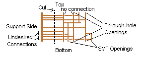
Interestingly, this brings to mind another variation on the above method: instead of cutting each undesirable support connection, have all the support connections cross through a specific cross section, which is to be cut, severing all the undesirable ties. I illustrated it in MS Paint (quick and dirty). This would actually probably be a very cool option, and even though it looks like it would be wasteful of copper and have extra leads hanging around inside the board, the distances were exaggerated, and board design could be such as to minimize extra traces (and make it more artistic, even though the amount of copper and space wasted would be small and you wouldn't see the waste from the outside of the board). The diagram may be a bit hard to see, as the smallest feature is one pixel wide. I suggest opening it in MS Paint and zooming in to 2x, 6x, or 8x (some other viewing programs may blur the lines [Edit 2: actually, if you click the link in Internet Explorer 7 and zoom in by using ctrl and the scroll wheel or ctrl and +, it kinda looks ok]).
CCB.bmp
So anyway, this single cut (or possibly multiple cut, as it may be necessary to have such support sides in more than one location; still not too many cuts though) can be performed by any variety of simple implements, like scizzors, knives, lasers, etc (it would be really cool if I could get the shapes just right such that it becomes possible to breakaway by hand). It can be automated or not (if you don't do the rest of the process automated, then you probably wouldn't automate this last cut). Anyway, after you cut off the side with the support traces, it may be preferable to cover them up (to prevent accidental shorts [this makes me think- it could be a great place to put jumpers] or just for aesthetics). This can be done by putting it back in a slightly bigger box, with extra length on the side perpendicular to the cut side (leaving an opening between the interior side of the box and the cut side), and then pouring more dielectric. This could be done after soldering if you're making a hybrid circuit (HIC), such that you can cover these support traces and cover the components at the same time.
Anyway, very exciting now that there's a feasible method for separating the support traces.
The biggest problem is still heating up the metal to pour it into the mold. There are various options for this, and we can really reach any temperature we want to (this is the 21st century), but I'd prefer a lower melting point material if possible, to limit the extra equipment necessary (so that perhaps we can make it more user-friendly and integrate it better with the main project). I thought about just using solder, which is essentially low melting point conductive material, but it occured to me that if we used the same solder for soldering then there could be some problems when soldering (I imagine you might heat up the board traces and get a disconnection inside the board, which would be bad). Ideally, you'd use an extremely low temp lead-free solder for soldering components and a standard low temp solder for the traces.
Solder simply refers to a few of the alloys of the candidate metals I mentioned earlier. The advantage of buying solder instead of buying the component metals and mixing them yourself is that they are already prepared precisely for our requirements (low melting temp, high conductivity) and are easily acquirable. It still may be preferred (at least for my eventual experimentation) to custom mix the alloy.
Comments?
Edit: I forgot to attach the diagram (maybe it was my subconcious telling me to not post it because it's such a terrible picture).
Edited 2 time(s). Last edit at 08/21/2008 05:12PM by Joshua Merchant.
Edit (before posting): I should note that I did come up with a solution down near the end, just in case you felt like not reading this [rambling] post.
If you RepRapped the individual connections, they would be rather flimsy (as a plastic and then as copper) and hard to keep in the correct positions relative to each other. There are ways around this, and I'm open to other ideas. Here are some I came up with.
First, there's the obvious option of doing it as one piece, with the undesirable connections above the surface of the board, and cutting the connections manually. I then thought about how to do this automatically, and milling was the first thing that popped into my mind. As I thought about this, it seemed a bit silly to go through the hassle of casting if you're just going to mill anyway.
Next, I imagined using support material (using the paste extruder or something) to support the split up traces when printing the pattern. The problem with this is that they have to be molded and cast into copper, and so the support would probably need to be removed at some point during this process, and I'm not quite sure how it would be possible to keep the shapes supported without the supports.
The one possibility would be that the support material is the material for the copper mold as well as being a good dielectric. The object would be printed (with traces split up and held together with support material) and then the main build material (the trace material) would be removed, and the copper poured right in. The board would then be done (with the support material as the board material, which is why I said it would need to be a good dielectric as well). It should be noted that perhaps the main build material should be used as the support for the traces, and the support material as the traces; the traces are the ones that need to be easily removed, and support materials seem to be selected for this easy-removal property.
Alternately, I suppose it could be possible without using the build/support material as the final board material if there was a way to replace the build/support material with another material such that the traces don't move...
Then I came up with the idea that instead of having a support material support the traces, why not have the traces support themselves? This is similar to the original idea, except that the traces are separate and each one can stand on it's own. They would be printed, and then placed into the molding box. The box would be notched such that the traces could be easily placed inside without manual alignment (the notches would hold the pieces in place). Similar notches would then be used throughout to hold individual pieces in place.
This method would be tedious; it may be feasible with a pick and place, though.
Alternately, you could just go with something similar to both the original idea and this last one, and have all these little pieces connected at the bottom by a thin rail (or rails) of copper so that they can be moved and molded etc. as a single piece. The rails would be exposed to the surface and cut at the end. This is probably the best option, even if it does seem a bit redundant (it really isn't, now that I think about it). Viable cutting methods are handheld wire cutters, automated wire cutters, a milling head, a laser, etc. A laser would probably be the best option, as it would allow really close cuts. It wouldn't be a big deal, though, as these connections can be routed away from the parts and spread to whatever size necessary for the cutting method.
Interestingly, this brings to mind another variation on the above method: instead of cutting each undesirable support connection, have all the support connections cross through a specific cross section, which is to be cut, severing all the undesirable ties. I illustrated it in MS Paint (quick and dirty). This would actually probably be a very cool option, and even though it looks like it would be wasteful of copper and have extra leads hanging around inside the board, the distances were exaggerated, and board design could be such as to minimize extra traces (and make it more artistic, even though the amount of copper and space wasted would be small and you wouldn't see the waste from the outside of the board). The diagram may be a bit hard to see, as the smallest feature is one pixel wide. I suggest opening it in MS Paint and zooming in to 2x, 6x, or 8x (some other viewing programs may blur the lines [Edit 2: actually, if you click the link in Internet Explorer 7 and zoom in by using ctrl and the scroll wheel or ctrl and +, it kinda looks ok]).
CCB.bmp
So anyway, this single cut (or possibly multiple cut, as it may be necessary to have such support sides in more than one location; still not too many cuts though) can be performed by any variety of simple implements, like scizzors, knives, lasers, etc (it would be really cool if I could get the shapes just right such that it becomes possible to breakaway by hand). It can be automated or not (if you don't do the rest of the process automated, then you probably wouldn't automate this last cut). Anyway, after you cut off the side with the support traces, it may be preferable to cover them up (to prevent accidental shorts [this makes me think- it could be a great place to put jumpers] or just for aesthetics). This can be done by putting it back in a slightly bigger box, with extra length on the side perpendicular to the cut side (leaving an opening between the interior side of the box and the cut side), and then pouring more dielectric. This could be done after soldering if you're making a hybrid circuit (HIC), such that you can cover these support traces and cover the components at the same time.
Anyway, very exciting now that there's a feasible method for separating the support traces.
The biggest problem is still heating up the metal to pour it into the mold. There are various options for this, and we can really reach any temperature we want to (this is the 21st century), but I'd prefer a lower melting point material if possible, to limit the extra equipment necessary (so that perhaps we can make it more user-friendly and integrate it better with the main project). I thought about just using solder, which is essentially low melting point conductive material, but it occured to me that if we used the same solder for soldering then there could be some problems when soldering (I imagine you might heat up the board traces and get a disconnection inside the board, which would be bad). Ideally, you'd use an extremely low temp lead-free solder for soldering components and a standard low temp solder for the traces.
Solder simply refers to a few of the alloys of the candidate metals I mentioned earlier. The advantage of buying solder instead of buying the component metals and mixing them yourself is that they are already prepared precisely for our requirements (low melting temp, high conductivity) and are easily acquirable. It still may be preferred (at least for my eventual experimentation) to custom mix the alloy.
Comments?
Edit: I forgot to attach the diagram (maybe it was my subconcious telling me to not post it because it's such a terrible picture).
Edited 2 time(s). Last edit at 08/21/2008 05:12PM by Joshua Merchant.
|
Re: Printed Circuit Boards August 22, 2008 03:32AM |
Admin Registered: 17 years ago Posts: 179 |
I've got another attempt at the lasercut RepRap going through. The problem is in making it economical. I'm at US$330 for the mechanical parts, and I think I can get it trimmed down a little further as the current run includes some experimental and hence duplicated parts.
There is also [bitsfrombytes] who are doing a lasercut set.
Vik :v)
There is also [bitsfrombytes] who are doing a lasercut set.
Vik :v)
|
Re: Printed Circuit Boards August 22, 2008 06:07PM |
Registered: 17 years ago Posts: 225 |
|
Re: Printed Circuit Boards August 29, 2008 10:18AM |
Registered: 16 years ago Posts: 438 |
How about this:
Three heads - plastic, solder, and pick'n'place, and a pot of molten solder with a layer of flux on the surface off to one side.
One of the problems with placing the components in the channels before solder is poured is flux. This could be solved by pre-tinning the components. pick them up with a vaccum + hypodermic needle based pickup head, dip them into the flux and down into the solder. Then you'd probably need to suck the excess solder off with a small vaccum system before placing it in the channel on the board and printing more plastic on top of it to hold it in place.
By pre-tinning the components and holding them in place with plastic, we can avoid leaving flux remanants in the final object. We also avoid "press fit" which not only requires manual intervention, but cannot embed components inside the plastic.
There are several possible sticking points with this scheme.
We need a flux that is liquid enough to shove the components through, and viscous enough that it won't get sucked up into our pick-n-place head in significant amounts. It also needs to be stable at the temperatures we're working at or be in a seperate tub. (meaning we'd have to dip the component twice)
Designing a vaccum system to suck the excess solder off may be non-trivial. Should be doable, as we have a working example in the common "solder sucker" used to desolder components in electronics shops across the world. Don't suck the component off the pick-n-place head though!
The components must be embeded into the channel in a way such that they are stable against the flow of solder into the channel, sealed against the solder flowing under, over, or around the component to short it out, and exposed enough that the surface tension of the solder doesn't prevent it's making contact with the pre-tinned ends. This may be complicated because the components don't exactly match (in several ways) the profile of the extruded channel minus a layer of plastic on top. We'll need to smear things somewhat, no doubt. We may also need to heat up the component itself - make it squoosh down into the existing plastic slightly.
And then there's chips. With multiple leads. And fine lead pitches (whats the term for that, anyway?) I'm envisioning using primarily surface-mount components for this stuff. To mount a fine-pitch surface mount chip this way we'd have to lay down lines of plastic that are narrow enough to be between the contacts. I think that works out to .2mm for the fine pitch surface mount stuff. And we haven't even mentioned the precision of placement required.
Still sounds doable, but we're a long way from easy. You'd be able to make some really, really small circuits though. Smaller and more closely packed than conventional surface mount technology even.
I really don't like the idea of press-fit stuff, except for batteries. Mostly, I admit, because I'm lazy and want a more automated process. And I really don't like the idea of laying out traces and solder components in by hand after the build is finished.
I of course, am speaking purely speculatively, as I'm still working on the polymer pump for my first repstrap.
--
I'm building it with Baling Wire
|
Re: Printed Circuit Boards August 29, 2008 11:32AM |
Registered: 16 years ago Posts: 900 |
I agree with you re Press Fit.
Like a lot of contact methods it is troubled by gas ingress and oxidization.
Wire wrap was always supposed to be a gas tight joint, experience of doing a bunch though and trying to use the kit at a much later date proved otherwise. No matter how good you were you always had to spend a bunch of time debugging the quality of the connections and over time the projects just got flakier. Even though metal migration through current transfer was again supposed to improve the joint. It never really did.
I still have a eurocard in my test rack that uses an Intel 8052AH Basic micro controller which I wire wrapped years ago. I have given up on it as the flakiness got too much in the end.
Even BT in the old exchanges (some pretty much still in use) wire wrapped then soldered as well.
aka47
Necessity hopefully becomes the absentee parent of successfully invented children.
|
Re: Printed Circuit Boards September 01, 2008 09:35AM |
Registered: 16 years ago Posts: 900 |
OK
Here's a design (built and documented) for a Universal Pen Holder and Touch Probe Tool Head
Blogged here:-
[builders.reprap.org]
Documented Here:-
[reprap.org]
I turned this out to help those folk who want to experiment with photo plotting or like greenarrow want to draw some etch/photo resist direct onto bare/pre-sensitised boards and play with prototyping PCB's this way.
Hope it's of value,
I am waiting for some motors and electronics from the RRRF before I can actually play with the prototyping and digitizing myself. But hope to catch up to those who can shortly.....
Cheers
aka47
Necessity hopefully becomes the absentee parent of successfully invented children.

Sorry, only registered users may post in this forum.