Gen 7 pin allocations
Posted by Grumpy Mike
|
Gen 7 pin allocations July 12, 2011 01:44AM |
Registered: 14 years ago Posts: 24 |
I am in the process of making a Gen 7 circuit on strip board. I used a Atmega 644 running at 20MHz. I have the processor down and I flashed in the boot loader yesterday using the arduino's built in ArduinoISP sketch. I put some red / blue LEDs on the step and direction inputs to each driver so I get red, blue and purple indication of the motor drives. These were all flashing away merrily with some test code. By the way I run a Mac.
However, I want to support an LCD display and SD card interface as well. Looking at the pin usage it seems there are some pins used for limit switches that will interfere with the SD card's SPI interface. There are also some unused pins on the processor. Chip pins 26 & 27 (logic pin 20 & 21) and chip pins 16 to 20 (logic pins 10 to 14). Also I don't think I will need logic Pin 15 with my power supply.
Finally what is the fan output used for? I am going to use the mini extruder that has a fan that runs continuously. So do I need this?
Does anyone know any reason for not allocating these pins to my desired extra functions. Of course I will have to change the pin definitions in the code and add some extra code.
|
Re: Gen 7 pin allocations July 12, 2011 03:59AM |
Registered: 13 years ago Posts: 7,616 |
Quote
Looking at the pin usage it seems there are some pins used for limit switches that will interfere with the SD card's SPI interface.
Yes, because without SD-card, there's no reason not to do this.
Quote
Finally what is the fan output used for?
For switching a fan on an off? Anyways, v1.3 has no longer a MOSFET for the fan.
Quote
Does anyone know any reason for not allocating these pins to my desired extra functions.
There is none. Unused pins are, well, not used. Free for other purposes.
| Generation 7 Electronics | Teacup Firmware | RepRap DIY |
|
Re: Gen 7 pin allocations September 11, 2011 03:05PM |
Registered: 12 years ago Posts: 16 |
Hi,
Thanks for all developers, great work!
I am very new in reprap and I am thinking similar details on my head.
I post this message to this topic, because I don't like to open new with same basic question.
I have now Generation7 schematics and PCB layout under EAGLE CAD.
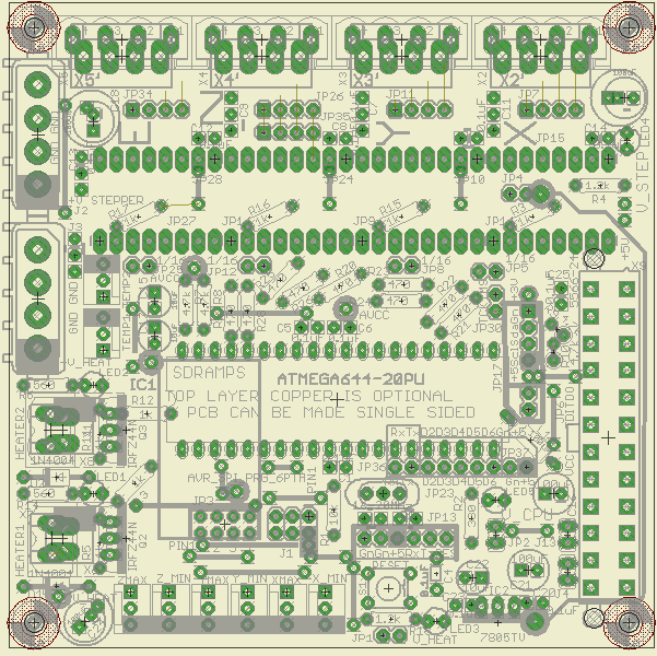
My PCB layout size is reduced to 10*10 cm and it is still makeable using toner transfer or photoresistive. Also milling is possible (actually I mill it with LPKF). PCB is single sided, all electrical features should be just like original 1.3.1 version, as far as I know.
SDRAM question has been laying around for a while so maybe it is not accepted or needed at all.. ??
But I like to inform that I allready have a PCB plan and some Eagle CAD files with following features (NOT tested at all):
1. Maybe a working possibility to use SDRAMPS. But NO formware.
MOSI, MISO and SCK signals are currently allocated for programming header. A second pin header is needed parallel to programming header due to their different pin layout, but that is not a problem for PCB layout.
SDRAMP Chip Select signal should be allocated too. Has anybody any idea which pin should be best to use for it?
And has anybody plan for software, may it never work at all?
Some limit switches should moved away, but luckily on most cases only 3 limit switches is needed at all.
Pin 5 of CPU is SS but it is already allocated for heater control. Pin 40 of CPU is now free, and it is just possible to connect to SDRAMPS header using a wire link. I'd like to keep things compatible with original Generation7 in all the way.
2. LCD and buttons? Any plans for them? My plan is to accept removed I2C pins and pins 26 and 27 to be used for LCD. With VCC and GND signals added to same single pin row connector is a good way to make LCD connection.
Myke Predko has solved LCD connection using only 2 wire:
[www.rentron.com]
Some reasonable amount of buttons can be read using only 2 pin and no extra IC at all - if some tricks are allowed (use caps to make some delays etc.). This arrangement keeps the original extension pins free.
3. I recommend to add GND and VCC to that currently unused extension header (pins 16-20 of CPU). Also tracks and pins for LM7805 regulator would be nice to have at least as option, if somebody has only higher voltage power supply without 5V at all (as I have, I am using 24V PSU for steppers and heaters).
4. Could it be best to use PC standby voltage for USB to keep the whole 5V circuits alive?
I mean that +5V for stepper controllers could also be alive all the time, because IF stepper controllers are not with their Vcc and CPU has Vcc, then STEP and DIR signals should have some protection resistors to prevent their input pin overcurrent in cace if the CPU is somehow outputting a high logic and stepper controller has no VCC.
I recommend to add series resistors to all control lines between CPU and steppers. Am I right?
5. My version of 10'10 cm PCB allows also some LEDs for power lines and also VCC and GND on same line with currently unused extension connector (CPU pins 16-20). This may help developing any future extension for real use?
6. Also MOSFET gates needs to have pulldown resistors, because IF CPU has three stated its outputs (at reset, startup, software fault), the FET should not be allowed to drift partially conductive state. Dissipation power may destroy it.
If these features are never propably to get alive (software?) and accepted by you folks, I'll keep my version as my own private hobby. But if they are needeed and accepted, I'll possibly develop my Eagle files for public.
PCB preorder for testing may become possible, about €5-6 each.
I am informing all of this because I hope some opinions of others, especially firmware developers.
Is all of this worth of doing at all?
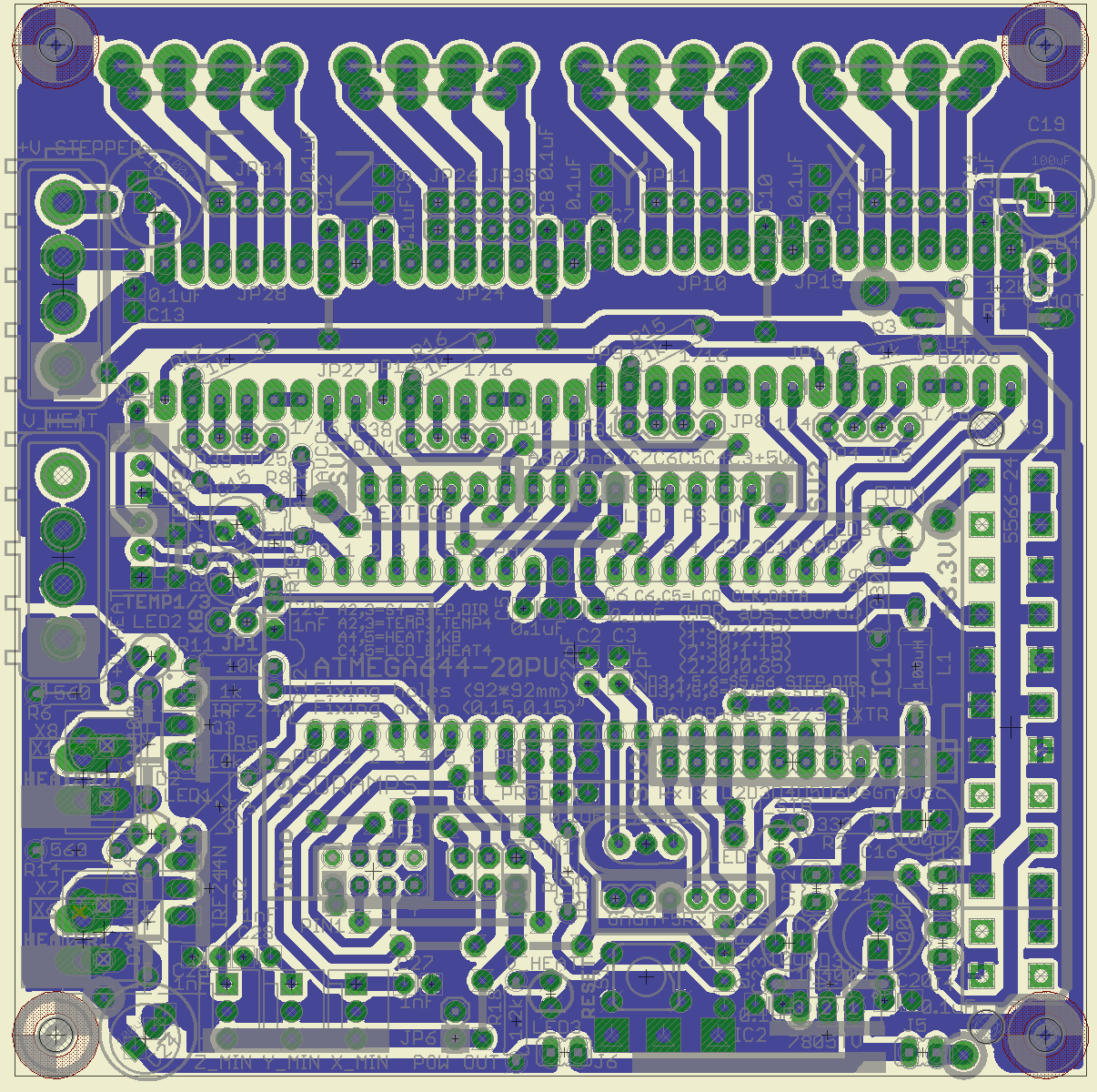
Attached is a picture of my current component placement.
Thanks for all developers, great work!
I am very new in reprap and I am thinking similar details on my head.
I post this message to this topic, because I don't like to open new with same basic question.
I have now Generation7 schematics and PCB layout under EAGLE CAD.
My PCB layout size is reduced to 10*10 cm and it is still makeable using toner transfer or photoresistive. Also milling is possible (actually I mill it with LPKF). PCB is single sided, all electrical features should be just like original 1.3.1 version, as far as I know.
SDRAM question has been laying around for a while so maybe it is not accepted or needed at all.. ??
But I like to inform that I allready have a PCB plan and some Eagle CAD files with following features (NOT tested at all):
1. Maybe a working possibility to use SDRAMPS. But NO formware.
MOSI, MISO and SCK signals are currently allocated for programming header. A second pin header is needed parallel to programming header due to their different pin layout, but that is not a problem for PCB layout.
SDRAMP Chip Select signal should be allocated too. Has anybody any idea which pin should be best to use for it?
And has anybody plan for software, may it never work at all?
Some limit switches should moved away, but luckily on most cases only 3 limit switches is needed at all.
Pin 5 of CPU is SS but it is already allocated for heater control. Pin 40 of CPU is now free, and it is just possible to connect to SDRAMPS header using a wire link. I'd like to keep things compatible with original Generation7 in all the way.
2. LCD and buttons? Any plans for them? My plan is to accept removed I2C pins and pins 26 and 27 to be used for LCD. With VCC and GND signals added to same single pin row connector is a good way to make LCD connection.
Myke Predko has solved LCD connection using only 2 wire:
[www.rentron.com]
Some reasonable amount of buttons can be read using only 2 pin and no extra IC at all - if some tricks are allowed (use caps to make some delays etc.). This arrangement keeps the original extension pins free.
3. I recommend to add GND and VCC to that currently unused extension header (pins 16-20 of CPU). Also tracks and pins for LM7805 regulator would be nice to have at least as option, if somebody has only higher voltage power supply without 5V at all (as I have, I am using 24V PSU for steppers and heaters).
4. Could it be best to use PC standby voltage for USB to keep the whole 5V circuits alive?
I mean that +5V for stepper controllers could also be alive all the time, because IF stepper controllers are not with their Vcc and CPU has Vcc, then STEP and DIR signals should have some protection resistors to prevent their input pin overcurrent in cace if the CPU is somehow outputting a high logic and stepper controller has no VCC.
I recommend to add series resistors to all control lines between CPU and steppers. Am I right?
5. My version of 10'10 cm PCB allows also some LEDs for power lines and also VCC and GND on same line with currently unused extension connector (CPU pins 16-20). This may help developing any future extension for real use?
6. Also MOSFET gates needs to have pulldown resistors, because IF CPU has three stated its outputs (at reset, startup, software fault), the FET should not be allowed to drift partially conductive state. Dissipation power may destroy it.
If these features are never propably to get alive (software?) and accepted by you folks, I'll keep my version as my own private hobby. But if they are needeed and accepted, I'll possibly develop my Eagle files for public.
PCB preorder for testing may become possible, about €5-6 each.
I am informing all of this because I hope some opinions of others, especially firmware developers.
Is all of this worth of doing at all?
Attached is a picture of my current component placement.
|
Re: Gen 7 pin allocations September 12, 2011 03:18AM |
Registered: 13 years ago Posts: 7,616 |
Looks good, Myke!
How is the programming interface of that? I see loops there, which will be interrupted up to 30'000 times a second. Does this work out with a 2 wire interface?
Ideally, this will become a connector for an extension board, stacked onto the base board similar to RAMPS. So we need not only GND and Vcc, but also a pin for the extruder's Enable pin (think of multiple extruders), SD card pins, I2C and perhaps a few others.
True.
That's mostly a matter of power usage. With the PSU going into standby by software, 5VSB will likely run 24 hours a day, so it shouldn't suck more power than really needed.
That's fairly often requested. I don't think you can destroy anything here, because if not in use, there's also no substantial current, but LEDs flickering around look just ugly. A thing which could be solved in software as well (put all unused pins to low).
You apparently moved miscrostepping jumpers more to the top, between Pololus and motor connectors. Does that really work out, on a single sided board?
Quote
Myke Predko has solved LCD connection using only 2 wire:
[www.rentron.com]
How is the programming interface of that? I see loops there, which will be interrupted up to 30'000 times a second. Does this work out with a 2 wire interface?
Quote
3. I recommend to add GND and VCC to that currently unused extension header (pins 16-20 of CPU).
Ideally, this will become a connector for an extension board, stacked onto the base board similar to RAMPS. So we need not only GND and Vcc, but also a pin for the extruder's Enable pin (think of multiple extruders), SD card pins, I2C and perhaps a few others.
Quote
Also tracks and pins for LM7805 regulator would be nice to have at least as option
True.
Quote
I mean that +5V for stepper controllers could also be alive all the time
That's mostly a matter of power usage. With the PSU going into standby by software, 5VSB will likely run 24 hours a day, so it shouldn't suck more power than really needed.
Quote
6. Also MOSFET gates needs to have pulldown resistors
That's fairly often requested. I don't think you can destroy anything here, because if not in use, there's also no substantial current, but LEDs flickering around look just ugly. A thing which could be solved in software as well (put all unused pins to low).
Quote
Attachments:
You apparently moved miscrostepping jumpers more to the top, between Pololus and motor connectors. Does that really work out, on a single sided board?
| Generation 7 Electronics | Teacup Firmware | RepRap DIY |
|
Re: Gen 7 pin allocations September 12, 2011 05:58AM |
Hi mikropehmo!
Interesting attempts ! I'm also planing to connect a LCD to my Gen7. For the button issue I thought about using the free ACD Pin PA0 in a way this Arduino LCD Shield works [www.nuelectronics.com].
I'm only want to display temperature and coordinates so this should only require minure changes in the firmware.
But first at all I have to have a deeper look on my Extruder Port on the board since 2 Pololus A4983 blew up :-/
|
Re: Gen 7 pin allocations September 12, 2011 11:13AM |
Registered: 12 years ago Posts: 16 |
Thanks for your rapid response!
I have made some track routing to consider thinking that this tiny PCb idea might be useful for real life.
Traumflug Wrote:
> Myke Predko.... How is the programming interface of that? I see
> loops there, which will be interrupted up to
> 30'000 times a second. Does this work out with a 2
> wire interface?
I have not tested this with any reprap code, but in old times, when I program with turbo Pascal (I AM old), I did made similar LCD idea. LCD loop can run interrupted or interlaced with stepper loop, because HD44780 LCD protocol is quite static. That means, it may not be any harm if LCD pulses are not timed at steady intervall.
> 3. I recommend to add GND and VCC....
>
> Ideally, this will become a connector for an
> extension board, stacked onto the base board
> similar to RAMPS. So we need not only GND and Vcc,
> but also a pin for the extruder's Enable pin
> (think of multiple extruders), SD card pins, I2C
> and perhaps a few others.
Good point. Stacked construction needs that mechanical layout of all necessary pins stays fixed mechanically during all the times.
Your example of SD card pins sharing (or what), does it mean that both processors (if stacked card has a processor) could or should controll same SD card? That sounds not good.
One simple solution to get freedom against any signal standardization could be here: to stack board together from CPU socket directly (plus PSU high current motor and heater cables, if needed).
So all next "generation" extensions uses CPU pins as connection point and extension board can contain new features limitless using original PCB as its signal interface. If both PCBs could be same sized they can be stacked using same (long) fixing screws. Spacing for existing cables must be arranged.
Concerning second stepper: could it be best if original Z stepper is reconfigured to drive that second extruder?
Then Z axle stepper is build again to new extension board. Z axle is stepped more rarely and it needs not so critical timing. Main control loop stay running at original CPU. Also Z axle can then be individually disabled when not in use and original enable line is not needed to feed out from PCB. One more stepper controller is needed anyway.
If CPU socket stacking method is used then there may not be any need to rearrange steppers. Simpy install another CPU card with more power over the existing CPU socket and go on.
But if second stacked CPU is not the selected way to go on, then signals for that additional stepper might be possible to arrange from original extension socket (or pins 26,27 ands one of I2C pin).
I kindly recommend that current extension socket is used for future extruder etc. features and those removed I2C pins + pin 26 and 27 could become reserved for "tiny extensions" like display and possible user panel interface with some possible jogging buttons etc. Why? ...well ....for layout reasons... ;-)
User panel lights (LCD backlight) could be controlled by PC PSU activation line, because that line is locating just under that pin strip socket (pin 21 of CPU). Also 3.3 V line is near to fed to same socket to give some feedback from PC PSU.
There is also JTAG pins among those pins, which may be more usefull on that area of use.
If SDRAM is possible to get operational using MISO, MOSI, SCK and maybe pin 40 for CS (has anybody done it yet?), then old version users can upgrade their connections guite easily with suitable cable. Rearranging end stoppers is needed, but first three of them (pins1-3) stays free even SDRAM would be in use.
> I mean that +5V for stepper controllers could also
> be alive all the time
I'll correct my own claim: according to datasheet, it may be OK to drop A498X Vcc voltage to zero and still feed logic high to their logic inputs.
Because input maximum voltage is mentioned to be 5.5V (guess that it is meant to be absolute voltage?), not anything like "Vcc + 0.3V" (which form is relative to existing Vcc)
So my protection resistors can be removed (but hard to find anything else to fill that area.. ;-D)
> You apparently moved miscrostepping jumpers more
> to the top, between Pololus and motor connectors.
No, those 4 pin rows are for optional pin strip stepper connectors just like RAMPS had. ...in my "intermediate" layout scheme, I had removed MS2 jumpers totally.... MS3 jumpers are just under pololus. With MS3 jumper only, the only selection is between 1/8 and 1/16 steps. Half stepping is lost. Does anybody really uses it?
I thought that half stepping might be useless for its low mechanical resolution.
Indeed that miss badly conflicts with combatibility. Because protection resistors are removed, MS2 jumper could be placed back.
On that scheme also termistor exitation is feeded from AVCC. That means possibility to keep thermistors alive with CPU using PC USB standby power only. That hope was on your own todo list for 1.4. I am originally "Microchip man", but I quess that also CPU core must kept alive too if thermistors (AD converters) are going to be read and results intelligently used anyvay?
That attached PCB planning idea was routed using 32 mills tracks and about 22-25 mills clearings.
Heater high current copper fills are minimum 190 mills wide on some short area. It should be enough.
PS. Just at the moment sending this message I noticed that scuba has needs for keyboard and LCD too. Must leave now so shortly:
AD converter is possible method to read maybe 5-10 buttons. I have used also another method: button line has a pullup resistor. Every button connects one diffrent sized capasitor to line. Then CPU resets capacitor and read time to logic high again. This timing measurement works if no ADC is available AND there is plenty of time to measure.
|
Re: Gen 7 pin allocations September 13, 2011 07:10AM |
Registered: 13 years ago Posts: 7,616 |
Quote
Your example of SD card pins sharing (or what), does it mean that both processors (if stacked card has a processor) could or should controll same SD card? That sounds not good.
Indeed, running multiple processors concurrently is a difficult task. That stacked card is more for pheripherals, like an USB connector, additional stepper drivers, SD card plugs, whatever people find useful. Processing all this is done on the main board.
Quote
Concerning second stepper: could it be best if original Z stepper is reconfigured to drive that second extruder?
I think it's safe to assume there's always only one extruder in use at a time. So you can turn one extruder off (enable pin) while the other is on. That said, Adrian is obviously with mixing extruders recently, which need multiple steppers on one extruder ...
Quote
If SDRAM is possible to get operational using MISO, MOSI, SCK and maybe pin 40 for CS (has anybody done it yet?)
Yes, at least one person is running a Gen7 with SD card. He re-wired two endstop pins and plugged the card into the programming header.
Quote
> You apparently moved miscrostepping jumpers more
> to the top, between Pololus and motor connectors.
No, those 4 pin rows are for optional pin strip stepper connectors just like RAMPS had.
I think it's safe to remove these big motor headers these days. Compatibility to Generation 3 Electronics is no longer an issue, all other modern electronics use Molex KK100 sized connectors and in general, motor currents have some tendency to go down instead of up.
Quote
Half stepping is lost. Does anybody really uses it?
Half-stepping is currently the only option on threaded rod axes in Teacup, for example.
Quote
On that scheme also termistor exitation is feeded from AVCC
At room temperature, the thermistor has 100kOhms, so that sucks 0.05 mA. Is this calculation correct? I'm not so bullet-proof at electronics.
Quote
That attached PCB planning idea was routed using 32 mills tracks and about 22-25 mills clearings.
Too bad you stick to closed source layout software,
 but I hope Gen7 can improve a bit from this anyways.
| Generation 7 Electronics | Teacup Firmware | RepRap DIY |
|
Re: Gen 7 pin allocations September 20, 2011 01:27PM |
Registered: 12 years ago Posts: 16 |
Traumflug Wrote:
> Too bad you stick to closed source layout
> software, but I hope Gen7 can improve a bit
> from this anyways.
You are right, I may be "stuck" on closed source (normally I use the most productivity CAD software I ever know, named Proteus) ;-)
This development I have made for practicing of Eagle Light software.
Light version restrictions are not problem, all routes are inside 80*100 mm area. Light version do allow produced PCB to be bigger and even routed outside that area. Only netlisted area is limited.
I used Eagle, because simply I didn't have any confortable feelings of the absolutely weird user interface of gEDA software. Definitely need to try to use and learn it more.
If somebody would be more familiar with it and interested in converting my proposals into real free life using gEDA, that would be very nice.
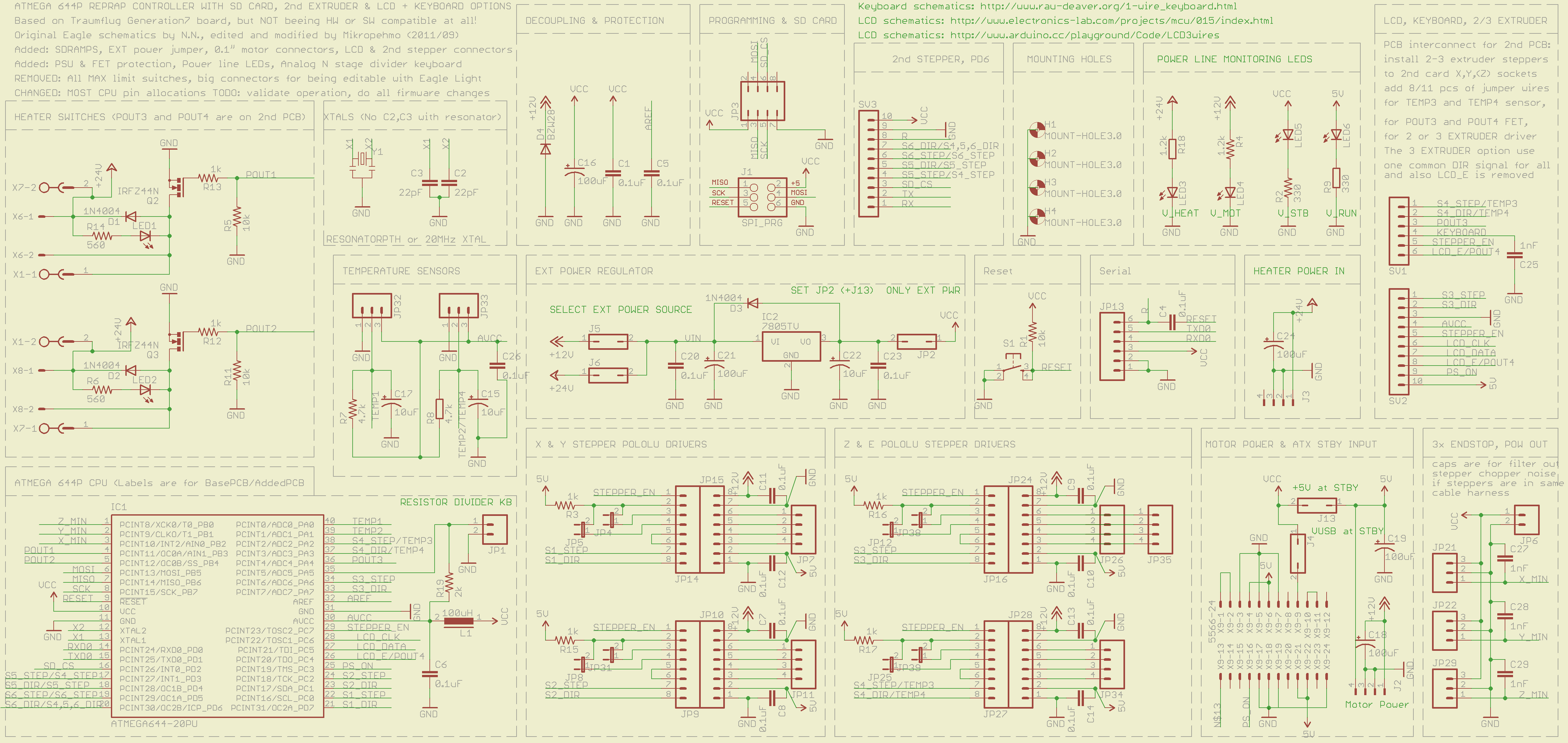
Attached is captured picture of one more possible schematics I have created. Now containing options for total 2 or 3 extruder steppers, 2+2 temperature measurement channels, 2+2 heater FET and one resistive divider keyboard (1-16 buttons) plus a LCD display using 2 wire connection.
Only LCD need some tiny PCB for shift register IC. It didn't fit on this PCB layout. ..yet...;-)
Also connector for SDRAMPS or my own similar SD Card reader is available among other candies I have added earlier.
Of course we all understand that this schematics and PCB is definitely not Generation7, so maybe it will be time to move it to another topic.
Honestly, I am not sure is it possible to develop a useful firmware for use all of these at all. Or will community ever need these features.
Now they are developed for the sake of being possible to route the PCB in 1 dm3 area and using only one layer only.
That is why I had to totally mess up previous CPU pin definitions.
If somebody like to try firmware development, it would be more than best favour.
Mechanically all doubled stepper, sensor and heater options are achived by connecting a second piece of similar PCB over base PCB. This stacked PCB is without CPU. Pin function rerouting is made by adding some wire links over the second PCB. Interconnection cables between PCBs are kept as pin to pin straight cables, so it is possible to stack PCB over each others.
That was the second point and idea of doing this learnfull Eagle brainwork...
Mikropehmo
> Too bad you stick to closed source layout
> software,
but I hope Gen7 can improve a bit> from this anyways.
You are right, I may be "stuck" on closed source (normally I use the most productivity CAD software I ever know, named Proteus) ;-)
This development I have made for practicing of Eagle Light software.
Light version restrictions are not problem, all routes are inside 80*100 mm area. Light version do allow produced PCB to be bigger and even routed outside that area. Only netlisted area is limited.
I used Eagle, because simply I didn't have any confortable feelings of the absolutely weird user interface of gEDA software. Definitely need to try to use and learn it more.
If somebody would be more familiar with it and interested in converting my proposals into real free life using gEDA, that would be very nice.
Attached is captured picture of one more possible schematics I have created. Now containing options for total 2 or 3 extruder steppers, 2+2 temperature measurement channels, 2+2 heater FET and one resistive divider keyboard (1-16 buttons) plus a LCD display using 2 wire connection.
Only LCD need some tiny PCB for shift register IC. It didn't fit on this PCB layout. ..yet...;-)
Also connector for SDRAMPS or my own similar SD Card reader is available among other candies I have added earlier.
Of course we all understand that this schematics and PCB is definitely not Generation7, so maybe it will be time to move it to another topic.
Honestly, I am not sure is it possible to develop a useful firmware for use all of these at all. Or will community ever need these features.
Now they are developed for the sake of being possible to route the PCB in 1 dm3 area and using only one layer only.
That is why I had to totally mess up previous CPU pin definitions.
If somebody like to try firmware development, it would be more than best favour.
Mechanically all doubled stepper, sensor and heater options are achived by connecting a second piece of similar PCB over base PCB. This stacked PCB is without CPU. Pin function rerouting is made by adding some wire links over the second PCB. Interconnection cables between PCBs are kept as pin to pin straight cables, so it is possible to stack PCB over each others.
That was the second point and idea of doing this learnfull Eagle brainwork...
Mikropehmo
|
Re: Gen 7 pin allocations September 20, 2011 02:30PM |
Registered: 13 years ago Posts: 1,352 |
I got proteus too, i just dont find it as easy as eagle. Probably others aswell - and this might account why eagle is fancy in diy community.
About the tone of extra feature, it would certainly be nice to have them, at least as provisions or options. Modularity is a great thing. Though if i would say 2 different extruders would be enough for now, afaik 2 physically different ones are not yet in practice, extra fets for fan+maybe some les on toolhead would be cool, LCD and buttons (simple ones, not resistive screen type) are nice. Shield or not, doesnt matter much.
I think in the big picture many things depends on if you want to orient it to DIY or to a board commercially made.
Because if its a board for DIY, then board space and layout doesnt matter, e.g. it can be spaced out, as big as needed, and even if half of it will represent just provisional space for some addons that arent going to be much used, it still doesnt matter. Extra board space for DIY boards is of no concern as additional cost of board space is that insignificant in DIY (at least how i see it). On the other hand if its destined to be made commercially, then every single square mm would matter and i believe it could add a price increase because such reprap orders are small and rare and spread, therefore prices are high as a result. I would rather go DIY at this point tbh, but thats just me, thinking that it would allow for faster development and iterations. Its also fairly easy later on to just squeeze things in to make a smaller layout once things have settled.
Are you up to put the sources on the wiki and document some basics? Also would that be GPL license or not?
|
Re: Gen 7 pin allocations September 20, 2011 05:23PM |
Registered: 12 years ago Posts: 16 |
Good points, NoodMan
.. Proteus have totally different mouse clicking principles than any other Windows based CAD, but when you get familiar with its logic, no one other CAD uses as less mouse clicks and cursor movements between menus for normal working tasks, thanks to its ability to "know" what your try to do.
At the very begining, to my eyes and hands, Eagle had totally horable UI, but now it seems to have at least some nice features ... :-)
Actually a question whether aPCB is possible to make DIY or not, is allmost not depending of area where a layout is spreaded. Allmost only thing is wire thickness, mostly pad sizes (which are most cases too small) and insulation clearances. Actually a smaller total area should be easier to made "in kitchen". 100*160 mm is a qood common standard.
90% of PCBs that I have seen are difficult to made DIY just only because people think that tiny pads (Eagle default uses just them!!) and huge clearances make things easier. Actually it is just opposite.
On Eagle I have not find any way to adjust components pad sizes on the fly. Maybe teh only way is to adjust them directly on library? In Proteus it is just one single click per pad!
Personally I like to stuff layout very tightly. But all this is off topic. Sorry.
Reason for making PCB just exactly 1dm3 is that some commercial companies make very (some $) cheap PCBs if they are just that size. One mm more and bang, price will be doubled.
This size PCBs can be ordered cheaper than one can get same amount of bare FR4 laminate - only pitfall it that you'll get 10 of them...
License would have to be same as other reprappers may have, I guess? It might be quite bad act if somebody will close ideas that have been developed in free community. I have not studied that yet. Of cource my personal favourite is to be able to sell at least some PCBs, but earning any real money for living is beyond my highest hope of gold anyway. ;-(
First I'll try to adjust some suitable firmware to accept this pin configuration and then I'll have some base to set errorfree files and documents to more public (wiki things I have never before done ... shame, I may be too oldschool guy...)
Be free to give opinions and help developing firmware. A batch of PCBs for testing will be made or ordered soon.
|
Re: Gen 7 pin allocations September 20, 2011 06:08PM |
Registered: 13 years ago Posts: 1,352 |
Yup in eagle in order to change the pads one would need to edit the library, and usually means making another pad/size/name, because a certain pad footprint could be used by more than one ic in that lib, so if you change the default, that will change it for all parts that use that package. Which may be your intent or not. I think is common for a project that is fairly complex, to have a dedicated library with everything that is not standard inside.
About general layout, i also think that smaller is easier, so i much prefer smd over trough hole, and the only pads i wanted to change were tqfp ones and the 1206 footprints in order to be able to squeeze easier a thicker route in between them (which is fairly common). For r and c smds i made a new package or sometimes i use bigger pads if needed, and for the tqfp pads i typically use a dumb approach like edit the image in an editor and insert white square rectangles in between. That is because i like toner transfer, and for iteration purposes, image editor changes feel somehow easier to do (scale+%). In rest i find everything including tqfp pins very much easy to do. In principle, i wouldnt pay just for a pcb board because i would rather just do it myself.
I believe we are kinda off-topic at this point, so for respect to this particular thread and its major contributors, i would suggest to wrap up it here, and continue some other place and probably some other time. Cheers!
|
Re: Gen 7 pin allocations September 15, 2012 07:21AM |
Registered: 11 years ago Posts: 121 |
|
Re: Gen 7 pin allocations September 16, 2012 05:03AM |
Registered: 13 years ago Posts: 7,616 |
There is no Gen7 "Eagle version". Somebody made a derivate which does many things differently, which is fine, but he also named it "Gen7", which is plain wrong.
| Generation 7 Electronics | Teacup Firmware | RepRap DIY |
|
Re: Gen 7 pin allocations September 17, 2012 10:11AM |
Registered: 11 years ago Posts: 121 |
Hi
Sorry if I stirred it up... I was referring to the one shown above.
I do value your Generation 7 as the true Gen 7. I would be lost without it...
If you'd prefer, I can open a new thread with my suggestions? Rather than forking, it makes more sense to incorporate changes.
- AVR-CDC for USB-TTL (I have a tested working implementation)
- Physical layout tweaks.
Peter
|
Re: Gen 7 pin allocations September 18, 2012 05:58AM |
Registered: 13 years ago Posts: 7,616 |
Quote
If you'd prefer, I can open a new thread with my suggestions?
Thanks for the offer, but this isn't neccessary. Now everybody knows what's going on.
Quote
Rather than forking, it makes more sense to incorporate changes.
- AVR-CDC for USB-TTL (I have a tested working implementation)
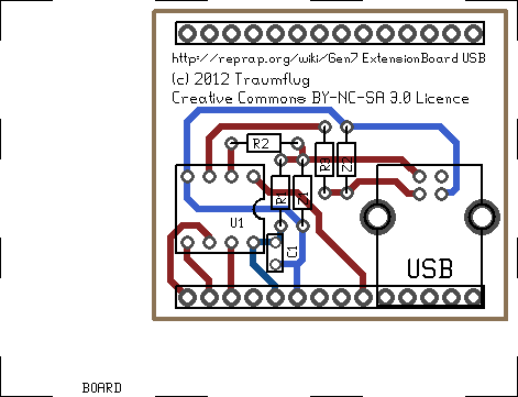
Very true. Seeing your design I made my own, for now on an extension board (can be integrated later):

As you can see, it uses an 8 pin ATtiny. The idea is to use SPI for ATmega <-> ATtiny communications. If the electronics controls both ends of the communications line, there's no need to stick with the slow/demanding RS-232 protocol. This would even allow to program factory-fresh ATmegas if the ATtiny is programmed to do both, act as a programmer as well as a plain serial communicator. Should be doable.
What do you think?
| Generation 7 Electronics | Teacup Firmware | RepRap DIY |
|
Re: Gen 7 pin allocations September 18, 2012 06:16AM |
Registered: 11 years ago Posts: 121 |
Exactly what I have been planning.
Just one problem: The ATtiny 45 only supports 4800 Baud. Use a 2313 at 16Mhz then you have DTR for autoreset, and also 38400 Baud. I have mine working quite well with this.
See [github.com] (sorry it's in Eagle - someday I might go through the schlep of learning gEDA...) - I found a nice space to integrate it without moving too many things around... On lower left corner. There is PNGs too so you dont have to download Eagle.
In terms of using it for SPI - I think rather take the effort and etch a small VUSBtiny board like my tinyduino (http://www.itux.co.za/2012/08/using-a-tinyduino-to-program-any-avr-even-surface-mount/ and [www.itux.co.za]) - singlesided... It's not like you touch the bootloader more than once (really...)
So one of two options: integrate the 2313 like I already have or make a 2313 expansion header? Just one note, the DTR pins in me and cmrdkeen.net's CDC firmware is in a different pin than the default...
Personally I vote for integrate, then the next thing I'd like to use the expansion for is lcd/sd...
Peter
|
Re: Gen 7 pin allocations September 18, 2012 08:08AM |
Registered: 13 years ago Posts: 7,616 |
Quote
The ATtiny 45 only supports 4800 Baud.
Yes, that's true. Because the RS-232 timing protocol is so demanding and the smaller ATtinys have no hardware UART. A synchronous protocol supported in hardware should work much faster. Like SPI or TWI/I2C. In theory, SPI supports communications speeds up to CLOCK / 2, right? That'd be 16 MHz / 2 = 8 Mbit or equal 9'000'000 baud. Compare that to the lame 250'000 baud others are doing

Quote
it's in Eagle
No worries. I have Eagle installed already. I just see no reason to use it, as it's closed source and size-constrained. Moving from Eagle to gEDA is probably mostly a matter of getting new habits, the feature set for our level of complexity is easily covered by both.
Quote
Personally I vote for integrate
Sure. It's just not important at this point in time and modifying an extension board for development is much simpler than soldering an entire main board each time. Things spinning in my head are:
- how to get Teacup/other firmwares to do SPI communications
- how to make a combined programmer/communicator firmware
- how to handle this V-USB thing, for beginners it looks like voodoo
- which USB protocol is supported by V-USB and also unleashes the speed of the available hardware
- which adjustments are required for pronsole/printrun/pronterface and Debian/Windows/Mac OS X
- how to get these adjustments into all the firmwares (a likely difficult task, as the development community strongly favours the RAMPS/Marlin combo)
- how to document all this in a way newbies can work with?
Likely the answers are all there, yet, I just have to find them.
| Generation 7 Electronics | Teacup Firmware | RepRap DIY |
|
Re: Gen 7 pin allocations September 18, 2012 08:12AM |
Registered: 11 years ago Posts: 121 |
Well I think Gen 7 v 1.7 can focus on the SPI and other ideas that will need to be adopted by OS/GCode senders and firmware...
I think a good course of action:
1.4.2 = 1.4.1 with a USB-TTL AVRCDC Expansion board. Not a lot of voodoo. I can provide a Arduino cores/boards that will burn AVR CDC to a 2313.
This will give us a bit of testing time... No major changes, we can do it right away as this is still serial.
If testing prove is to work as it did for me, 1.5.0 can have it integrated....
PS: Shout if you need any help, I'm at your beck and will
[edit]
- how to document all this in a way newbies can work with?
At least that much you have down to a tee... I was a beginner when I built my first gen 7... its the first electronics I used myself... And your style of documentation was a pleasure to follow. Built a few at the local hackerspace as well, pop the wiki up on screen and let everyone go to town. no questions...
[/edit]
Peter
Edited 1 time(s). Last edit at 09/18/2012 08:23AM by peter6960.
Sorry, only registered users may post in this forum.